How to Copy PCB Design Yourself

Copying PCB Design, also known as PCB Reverse Engineering, simply saying, is to firstly scan the the board to be copied, record the detailed location of the components. Then remove the components to make a bill of materials (BOM). After that arrange material procurement,  bare board is scanned into the image copy board software Processing and reverting to PCB board image file, and then sending the PCB file to PCB factories for sampling. 

Specific technical steps are as follows:


1. The first step, get a printed circuit board, first of all recording on paper for all the components of the model, parameters, and location, especially the diode, transistor direction, IC notch direction. It’s better to use a digital camera to take two photos to record  components location. A lot of PCB circuit boards are getting more and more complex, and the diode diodes on top may be neglected sometimes when you do not pay enough attention when checking them by raw eyes.


2. The second step, remove all the components, and remove the tin from the PAD hole. Clean the PCB with alcohol and put it into the scanner. The scanner needs adjust to a little more high pixels to get a clearer image. Then re-use water yarn paper to the top and bottom slightly polished, polishing until the copper film shiny, into the scanner. Start PHOTOSHOP, color the two layers were swept in. Please note that the PCB must be placed in a horizontal and vertical position in the scanner, otherwise the scanned image will not work.


PCB Clone Services

Full integrated PCB cloning service at one place @Chinapcbcopy.com

    #1. IC Unlock + PCB Reverse engineering Services

    #2. Fast PCB / PCBA Prototype

    #3. Prototype testing & error correction

    #4. Engineering files correction per testing result

    #5. PCB / PCBA Re-production
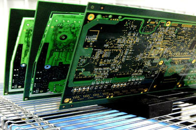

3. The third step is to adjust the canvas contrast, brightness, so that part of the copper film and non-copper film contrast strongly, and then change the secondary map to black and white color, check the lines are clear, if not clear, repeat this step. If clear, the picture will be saved as black and white BMP format files, TOP BMP and BOT BMP, if you find that there are problems with graphics, PHOTOSHOP can also be used for fix and correction.

4. Next, the two BMP format files were converted to PROTEL format file transferred into the PROTEL two layers. If two layers of PAD and VIA basically overlap, it indicates that the first few steps to do well. If If there is deviation, repeat the third step.

(PCB copy board needs to be very patient, because a small problem will affect the quality and copy board after the match.)

5. Then, you could convert the top-level BMP to the TOP PCB. Please note that the conversion to the SILK layer is the yellow one, and then you are tracing the top-level and placing the device according to the second-step drawing. SILK deleted after painting. Repeat until you have drawn all the layers.

6. In the PROTEL, you need to import TOP PCB and BOT PCB, and  emerge  into  one file.

7. Use laser printer to print out  TOP LAYER, BOTTOM LAYER as transparent films (1: 1 ratio). Place the  films on  the PCB copper layers, compare the error, if not, you’re done.

A PCB Design now has been copied from the original board. But it was done in half. After testing the electronic performance of the copied board, and  if it’s same as the original board. 

For multilayer board copy, you need to be very carefully polishing to the inner layer, then repeating the third to fifth copy board steps. Of course, the name of the graphic is also different. Generally, 2 layer PCB copy  is much simpler than multi-layer board. It’s common to have misalignment issues if you are not experienced on Multi-layer board copy. For high layer PCB, there was a lot of Plated Thru Holes, and Non Plated Thru Holes. The differences of the holes are very small, so some the conductivity will be messed up if you made any mistakes at this stage for high layer boards copy.

There are a lot of other methods for delayer   multi-layer PCBs. Apart from manually sanding, we also suggest sand blasting machine, CNC milling machine to delayer  the inner layers. 3D  X-ray is also  a very effective way to obtain the drawings for multilayer PCBs, if you can get access to 3D X-ray machine.

Source from Fast PCB Studio
www.chinaPCBcopy.com

How to Copy PCB Design Yourself | Fast PCB Studio

How to Copy PCB Design Yourself

Published by Fast PCB Studio on

How to Copy PCB Design Yourself

Copying PCB Design, also known as PCB Reverse Engineering, simply saying, is to firstly scan the the board to be copied, record the detailed location of the components. Then remove the components to make a bill of materials (BOM). After that arrange material procurement,  bare board is scanned into the image copy board software Processing and reverting to PCB board image file, and then sending the PCB file to PCB factories for sampling. 

Specific technical steps are as follows:


1. The first step, get a printed circuit board, first of all recording on paper for all the components of the model, parameters, and location, especially the diode, transistor direction, IC notch direction. It’s better to use a digital camera to take two photos to record  components location. A lot of PCB circuit boards are getting more and more complex, and the diode diodes on top may be neglected sometimes when you do not pay enough attention when checking them by raw eyes.


2. The second step, remove all the components, and remove the tin from the PAD hole. Clean the PCB with alcohol and put it into the scanner. The scanner needs adjust to a little more high pixels to get a clearer image. Then re-use water yarn paper to the top and bottom slightly polished, polishing until the copper film shiny, into the scanner. Start PHOTOSHOP, color the two layers were swept in. Please note that the PCB must be placed in a horizontal and vertical position in the scanner, otherwise the scanned image will not work.


PCB Clone Services

Full integrated PCB cloning service at one place @Chinapcbcopy.com

    #1. IC Unlock + PCB Reverse engineering Services

    #2. Fast PCB / PCBA Prototype

    #3. Prototype testing & error correction

    #4. Engineering files correction per testing result

    #5. PCB / PCBA Re-production

3. The third step is to adjust the canvas contrast, brightness, so that part of the copper film and non-copper film contrast strongly, and then change the secondary map to black and white color, check the lines are clear, if not clear, repeat this step. If clear, the picture will be saved as black and white BMP format files, TOP BMP and BOT BMP, if you find that there are problems with graphics, PHOTOSHOP can also be used for fix and correction.

4. Next, the two BMP format files were converted to PROTEL format file transferred into the PROTEL two layers. If two layers of PAD and VIA basically overlap, it indicates that the first few steps to do well. If If there is deviation, repeat the third step.

(PCB copy board needs to be very patient, because a small problem will affect the quality and copy board after the match.)

5. Then, you could convert the top-level BMP to the TOP PCB. Please note that the conversion to the SILK layer is the yellow one, and then you are tracing the top-level and placing the device according to the second-step drawing. SILK deleted after painting. Repeat until you have drawn all the layers.

6. In the PROTEL, you need to import TOP PCB and BOT PCB, and  emerge  into  one file.

7. Use laser printer to print out  TOP LAYER, BOTTOM LAYER as transparent films (1: 1 ratio). Place the  films on  the PCB copper layers, compare the error, if not, you’re done.

A PCB Design now has been copied from the original board. But it was done in half. After testing the electronic performance of the copied board, and  if it’s same as the original board. 

For multilayer board copy, you need to be very carefully polishing to the inner layer, then repeating the third to fifth copy board steps. Of course, the name of the graphic is also different. Generally, 2 layer PCB copy  is much simpler than multi-layer board. It’s common to have misalignment issues if you are not experienced on Multi-layer board copy. For high layer PCB, there was a lot of Plated Thru Holes, and Non Plated Thru Holes. The differences of the holes are very small, so some the conductivity will be messed up if you made any mistakes at this stage for high layer boards copy.

There are a lot of other methods for delayer   multi-layer PCBs. Apart from manually sanding, we also suggest sand blasting machine, CNC milling machine to delayer  the inner layers. 3D  X-ray is also  a very effective way to obtain the drawings for multilayer PCBs, if you can get access to 3D X-ray machine.

Source from Fast PCB Studio
www.chinaPCBcopy.com

Back to top