Fast PCB Studio
PCB Reverse Engineering
What is PCB Reverse Engineering

PCB reverse engineering is also known as PCB Copy, PCB cloning or PCB duplication. It is a reversely researching technology based on exisiting physical PCB boards.
PCB reverse engineering, that is, under the premise that there are already physical objects and circuit boards of electronic products, the reverse analysis technology is used to reversely analyze the circuit board, and the original product PCB file, bill of materials (BOM) file, schematic file, as well as the other production documents, such as PCB Gerber and PCB silk screen. Then use these engineering documents and production documents for PCB re-production, component soldering, flying probe test, circuit board debugging, in order to complete the entire copy of the original circuit board as sample.
Since electronic products are all composed of various types of circuit boards that form the core control part, the process of using PCB reverse engineering can realize the extraction of complete engineering materials of many electronic products already on the market, as well as the imitation of electronic products cloning.
How PCB Reverse Engineering would help PCB design & development
PCB reverse engineering is a reverse research technology that uses a series of reverse research techniques to obtain a PCB design, circuit schematic and a BOM for an existing & matual electronic design. A new product development that used to take two or three years to develop, now through reverse engineering technolgy, may take only a few months to complete.
In the past decade, the development of electronic technology has been changing with each passing day, and many electronic products have been upgraded at least once a year. Future electronic product updates may be faster. Many electronics engineers have felt that simply using conventional R&D methods can no longer meet the fast steps of modern electronic product replacement, and since there have been millions of matual design in the market, reverse engineering becomes an approach to fast adopt the market pace and catch up the top runners.
PCB Reverse Engineering Services
- PCB Gerber File
- BOM List
- Schematic Diagram
*PCB bare board will be delayered during the procedure and the sample PCB will no longer be able to reuse.
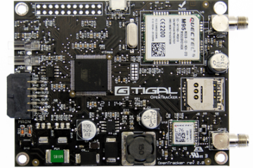
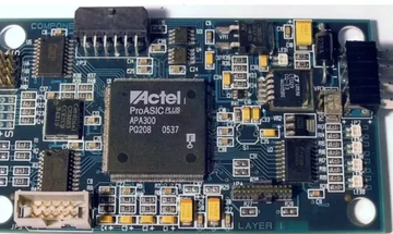
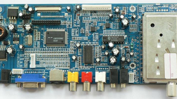
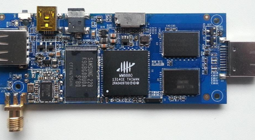
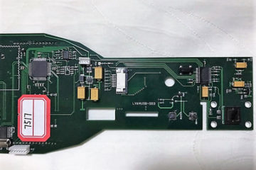
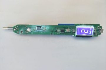
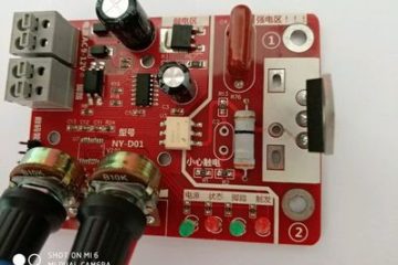
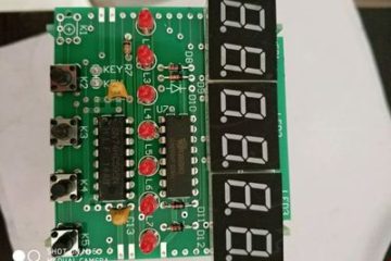
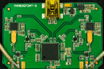
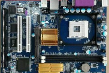
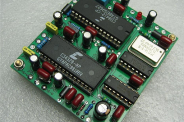
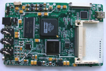
How to reverse engineer A PCB Board
In the age that there was no software for PCB reverse engineering, you can only reply on drawing and measuring with the caliper. The speed was slow and the accuracy was quite poor. Nowadays, it is very simple to use the software to reverse engineer multi-layer plated through hole boards.
Generally, you can scan or photograph the PCB board first, then load the picture into the software, and then copy it with the protel99. After patching, it can be dumped into a protel99 compatible format. The difficulty of the work will be from the PCB file converting to the schematic diagram. It needs to have rich experiences to have this part of work being completed as expected.
The precise method is to remove all components and record all component parameters and components. Corresponding to the number of screen printing layers one by one, after retaining the original data, then taking pictures or scanning the bare PCB board, the obtained photos or scanned images are loaded into the software, the software is different, the photo format requirements are different, and the oversized photo files will be too large that would affect the speed of loading in software, so large PCB board can be divided into several small pieces for copying, and then flattened. After the upper and lower layers are completed, the finished layer on the surface can be sanded with sandpaper, and the inner layer is gradually exposed, and a layer is applied and the layer is further polished until all is completed.
There are a lot of professional PCB reverse engineering companies, such as Fast PCB Studio in the industry, which can help you complete the complicated PCB board reverse engineering, and cloning. For some simple boards, it would also be a good experience to reverse engineer them by yourself. Today, we would like to share with you the basic techniques to reverse engineer a multi-layer plated through hole board.
Equipment required: Scanner, computer, PORTEL99 and AUTOCAD software required.
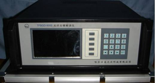
Equipment required: Scanner, computer, PORTEL99 and AUTOCAD software required.
Reverse Engineering Overview
Here is the short viedio of an overview of a PCB reverse engineering project, and the engineering file outcomes as an example:
PCB Delayer
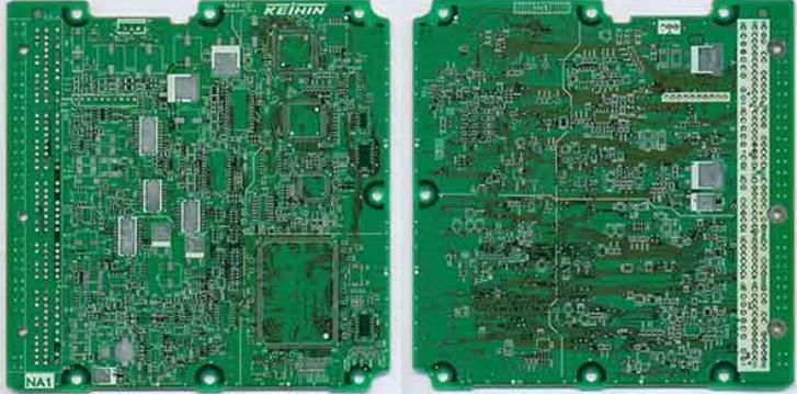
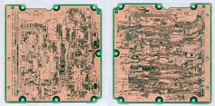
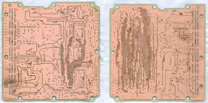
There are many ways to delayer a PCB now, such as x-ray scanning, chemical corrosion, Sandblasting, manual sanding etc.. Sanding will still be the most reliable and accurate way to complete the task.
Just use the example of manual sanding, when we finish sanding the top layer of the PCB, we usually use sandpaper to polish the surface layer to show the inner layer. The sandpaper can be the ordinary sandpaper sold in the normal hardware store. You need to use finer sandpaper when you start to sand the inductive layers. Generally, the PCB is tiled, then the sandpaper is pressed and rubbed evenly on the PCB. (If the board is small, you can also flatten the sandpaper and use a finger to hold the PCB and rub it on the sandpaper). The point is to flatten out so that it can be evenly ground.
Silk screen and solder mask are generally to be wiped off easily. When you see copper layer, you could change the sandpaper to finer ones as copper layer may be sanded of by a few times sanding with rougher sandpaper. For high layer PCBs, e.g. 6+ layers, it would normal have 2+ cores in the middle, it will take longer time to sand off. Bluetooth board can be done in 10 minutes, and the memory stick takes about 20-30 minutes.
PCB file Creation
1. Put the PCB board you want to copy into the scanner, start the scanner, and adjust the brightness and contrast in the scanner.
2. Open the AUTO CAD software, create a new CAD file, select Insert bitmap image in the inserted menu, and after selecting the image you want to insert, the Insert Image dialog box will appear. Select a ratio of 1:1 in the dialog box.
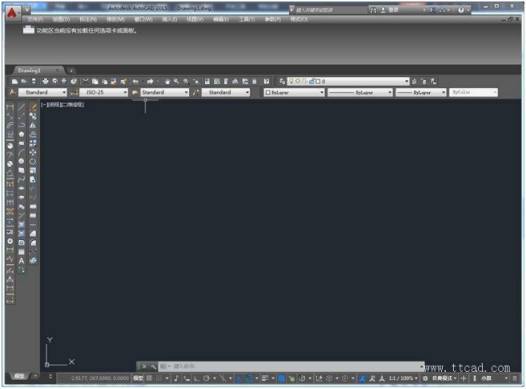
3. After inserting the PCB image, draw a rectangular frame to cover the border of the PCB. Note that when you draw the border, you should use the object to track the object. If you do not draw a border, the image is in the process of drawing the route. If you accidentally move, you can hardly register.
4. Draw the component package. Since the component package used in the PCB board we are copying does not necessarily match the component package in PORTEL99, we have to build the component package ourselves, that is, the shape of the component in the PCB we want to draw is drawn. When drawing component packaging, we must first count how many kinds of packages are used on the PCB. Each package only needs to be painted one. After all the packages are painted, we must transfer them to PORTEL 99 for processing. .
5. Open PORTEL99, first create a new PCB file, then import the CAD file in the file menu of the PORTEL99 PCB editor, and import the CAD file with the component model. After the import is successful, the PORTEL 99 PCB editor appears. The basic graphics of the component package.
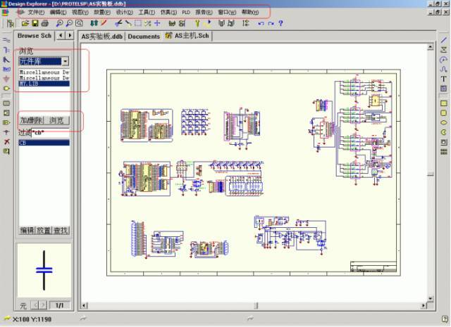
6. Create a new PCB component editor in PORTEL99, and then open the PCB component editor. After creating a new component, select a component package from the PORTEL99 PCB editor and copy it to the PCB component editor for component creation.
7. Once all component packages have been fabricated, place them in the PORTEL99 PCB Editor and export them as a CAD file.
8. After opening the CAD file of the component package drawing, open the CAD file that was previously imported into the PCB image, and copy the component package drawing to the CAD with the PCB image. At this time, close the CAD file with only the component package drawing. Just work in the CAD file with the PCB picture, arrange the components according to the angle and position of the components of the PCB diagram, and pay attention to making more sub-components by copying and pasting.
9. Place the pads and vias: After placing the component package, the next job is to place the pads and vias. First measure the inner and outer diameters of the pads in the CAD, then select the circle in the drawing menu. Sub-item, and determine the inner and outer diameter of the ring, the pad of the same size should be placed at one time when the pad is placed, but the square pad and the polygon pad cannot be placed, although it can be filled in CAD. The method fills the polygon into a solid, but the filled entity will only have an empty border when it goes inside PORTEL 99. Therefore, if there is a polygon pad in the PCB, we can use the line to trace the edge of the pad and go to Put the corresponding pads in PORTEL99.
10. Draw the trace: After the pad is drawn, start drawing the trace. The draw trace is drawn by the aggregate line. In the drawing menu, select the aggregate line to determine the start width and end width of the aggregate line. Start drawing. In the drawing process, if it is a straight line, you should select the orthogonal trace. If it is 45 degrees or other angles, you should cancel the orthogonal trace. If the width of the entire line is only a few specifications, we You can also draw with ordinary lines, but different line widths use different layers, go to PORTEL 99 and edit the line width.
11. When the line is completed, we will carry out the last work in the CAD, place the silk screen, if it is text, use the method of placing the text box. If it is irregular silk screen, use the polymerization line, of course. You also draw directly with lines, go to PORTEL 99 and edit the line width.
12. After the above steps, you have basically completed the work in CAD. If you don’t go to PORTEL, you can also ask the PCB manufacturer to help you make the board. You can also print out the layers you need and make your own. PCB, of course, the ultimate goal of my writing is to tell the reader to transfer the depicted graphics to PORTEL, so we will continue with the following steps.
13. Open the PORTEL99 PCB Editor and import the CAD files you have already drawn. Note that it is important to map the various layers of CAD to the various layers of PORTEL99 in the dialog box for importing files, regardless of your layer in CAD. What is the name, but you must know what layer this layer responds to in PORTEL99. If you do not control the chaos, you will spend more time on the PORTEL 99 layer conversion, and also when importing The default line width is also best changed.
14. Finally edit, after importing PORTEL99, we also need to make proper editing. For example, when we import, we put the lines and pads on the TOP LAYER layer. At this time, you should put all the pads on the MULTI LAVER layer. Also, no matter which angle you put the silkscreen text in CAD, you will be corrected when you go to PORTEL 99. At this time, you have to adjust it against the physical PCB.
15. If there is another line or silk screen, just follow the above method, then lead to the integration in PORTEL 99, pay attention to mirroring. Finally, check the image or PCB carefully, you can also make appropriate modifications. You’re done.
Precautions:
If you accidentally move the picture in CAD, then all the lines you draw will be invisible. At this time, you have to remove all the pictures, and then select all the lines you have drawn.
Schematic Creation
In PCB reverse engineering, PCB layout convert to schematic is the most difficult step to complete the whole reverse engineering work. It can be said that the previous preparation work is done for it.
There are also two ways to route: automatic layout and interactive layout. Before automatic layout, you can use interactive pre-layout traces that require more stringent requirements. The edges of the input and output should avoid adjacent parallel to avoid reflection interference.
Grounding should be added when necessary. The wiring of two adjacent layers should be perpendicular to each other, and parasitic coupling is easy to occur in parallel.
Step 1: Preliminary work of PCB schematic creation
1. Use the schematic design tool to draw the schematic and generate the corresponding network table. Of course, in some special cases, such as the circuit version is relatively simple, if you have a network table, you can also not design the schematic, directly enter the PCB design system, in the PCB design system, you can directly access the parts package, manual Generate a network table.
2. Manually change the network table. Define the pads that are not on the schematic diagram of the fixed feet of some components to the network connected to it. No physical connection can be defined to the ground or the protection ground. Change the pin names of the device names in the schematic and PCB package libraries to be consistent with those in the PCB package library, especially the diodes and transistors.
Step 2: Draw a package library of your own defined non-standard devices
It is recommended to put the devices you have drawn into a dedicated PCB library design file.
Step 3: Setting the PCB design environment and drawing the layout of the printed circuit board with hollowing in the middle, etc.
1. The first step after entering the PCB copy board system is to set the PCB design environment, including setting the grid size and type, cursor type, layout parameters, wiring parameters, and so on. Most of the parameters can use the system defaults, and after these parameters are set, it is in line with personal habits, and there is no need to modify them later.
2, planning the printed circuit board, mainly to determine the border of the circuit board, including the size of the circuit board and so on. Place the appropriate size pad where you need to place the mounting holes. Available for 6.5 to 8 mm OD and 3.2 to 3.5 mm OD pads for 3mm screws. Standard plates can be loaded from other boards or PCB izard.
Note: Before drawing the border of the board, be sure to set the current layer to the Keep Out layer, that is, disable the wiring layer.
Step 4: After opening all the PCB copy board files to be used, transfer the network table file and modify the part package.
This step is a very important link. The network table is the soul of the PCB automatic routing. It is also the interface between the schematic design and the impression circuit board design. Only when the network table is loaded can the circuit board be wired.
In the process of schematic design, the ERC inspection does not involve the packaging of the part. Therefore, when the schematic design, the package of the part may be forgotten, and the package of the part may be modified or supplemented according to the design situation when the network table is introduced.
Of course, you can manually generate a netlist directly in the PCB and specify the part package.
Step 5: Arranging the position of the circuit board copying component package, also called the component layout
Protel99 can be used for automatic layout or manual layout. If you are doing automatic layout, run “Auto Place” under “Tools”. With this command, you need to have enough patience. The key to wiring is layout, and most designers use manual layout. Select a component with the mouse, hold down the left mouse button, drag the component to the destination, release the left button, and fix the component. Protel99 adds some new tricks in layout. New interactive layout options include automatic selection and automatic alignment. Using the automatic selection method, components of similar packages can be quickly collected, then rotated, expanded, and organized into groups, which can be moved to the desired position on the board. When the simple layout is complete, use automatic alignment to neatly unfold or tighten a set of similar components.
Tip: When auto-selecting, use Shift+X or Y and Ctrl+X or Y to expand and contract the X, Y directions of the selected component.
Note: The layout of the parts should be considered comprehensively from the aspects of mechanical structure heat dissipation, electromagnetic interference, and convenience of future wiring. The devices associated with the mechanical dimensions are placed first, and these devices are locked, then the core components of the large positional devices and circuits, and then the small components of the periphery.
Step 6: Make appropriate adjustments according to the situation and then lock all the components
If the board space allows, you can put some wiring areas similar to the experiment board on the board. For large boards, add more screw holes in the middle. Screw holes should be added to the side of the device with heavy components or larger connectors. If necessary, put some test pads in place, preferably in the schematic. Change too small pad vias to define the network of all fixed screw pad pads to ground or protective ground.
After putting it in, use the VIEW3D function to check the actual effect and save it.
Step 7: PCB change board wiring rule setting
The wiring rules are the specifications for setting the wiring (such as the usage level, the line width of each group, the spacing of the vias, the topology of the wiring, etc.), which can be imported from other boards through the Menu of Design-Rules, and then imported into the board. This step does not have to be set every time, according to personal habits, set once.
Selecting Design-Rules generally requires resetting the following points:
1, safety spacing (Rearing label Clearance Constraint)
It specifies the distance that must be maintained between the trace pads of different networks on the board. The general board can be set to 0.254mm, the empty board can be set to 0.3mm, the dense patch board can be set to 0.2-0.22mm, and the production capacity of a few printing board manufacturers is 0.1-0.15mm, if it can be levied They can agree to you to set this value. Below 0.1mm is absolutely prohibited.
2, routing level and direction (Routing Labels Routing Layers)
Here you can set the trace layer used and the main trace direction of each layer. Please note that the single panel of the patch only uses the top layer, and the single panel of the inline type only uses the bottom layer, but the power layer of the multilayer board is not set here (can be used in the Design-Layer Stack Manager, after the top or bottom layer is used) Add Plane is added, double-click with the left mouse button to set, click this layer and delete with Delete), the mechanical layer is not set here (you can select the mechanical layer to be used in Design-Mechanical Layer, and choose whether it can be Whether the view is displayed in the single layer display mode at the same time).
Mechanical layer 1 is generally used for the border of the drawing board;
The mechanical layer 3 is generally used for mechanical structural members such as baffles on the drawing board;
The mechanical layer 4 is generally used to draw rulers and notes, etc., you can use the PCB Wizard to export a PCAT structure.
3, through hole shape (Routing label of Routing Via Style)
It specifies the inner and outer diameters of the vias that are automatically generated during manual and automatic routing. They are divided into minimum, maximum and preferred values. The preferred value is the most important, the same below.
4, the line width (Routing label Width Constraint)
It specifies the width of the traces for manual and automatic routing. The overall board range preference is typically 0.2-0.6mm, plus some network or network class (Net Class) linewidth settings, such as ground, +5 volt power line, AC power input line, power output line and power pack Wait. The network group can be defined in the Design-Netlist Manager in advance. The ground wire can be generally 1mm wide. The various power cables can be selected from 0.5-1mm width. The relationship between the line width and the current on the printed board is about 1 line per mm. The current of ampere can be found in the relevant information. When the wire diameter preference is too large, the SMD pad will automatically shrink to a trace between the minimum width and the width of the pad when it enters the SMD pad, where the board is the entire The line width constraint of the board has the lowest priority, that is, the line width constraint of the network and the network group is first satisfied when wiring. The figure below is an example
5, the setting of the copper connection shape (Manufacturing label Polygon Connect Style)
It is recommended to use the Relief Connect wire width Conductor Width to take 0.3-0.5mm 4 wires 45 or 90 degrees.
The rest of the items can generally be used with their original default values, and items such as the topology of the wiring, the spacing of the power planes, and the length of the network matching the connection shape can be set as needed.
Select Tools-Preferences, where the Interactive Routing of the Options column selects Push Obstacle (push other routes when encountering different network traces, Ignore Obstacle is traversed, and the Visual Obstacle is blocked) mode and select Automatically Remove (Automatically Remove). Remove extra traces). Track and Via in the Defaults column can also be changed, and you don’t have to move them.
Place the FILL fill layer in the area where you do not want to have traces, such as the heat sink and the wiring layer under the two-legged crystal oscillator. Place the FILL on the Top or Bottom Solder.
Wiring rule settings are also one of the keys to printed circuit board design and require a wealth of practical experience.
Step 8: Automatic routing and manual adjustment of printed circuit boards
1. Click the menu command Auto Route/Setup to set the automatic routing function.
Select all items except Add Testpoints, especially the Lock All Pre-Route option, and the Routing Grid can be 1mil or so. Before the automatic wiring starts, PROTEL will give you a recommended value and ignore it or change it to its recommended value. The smaller the value, the easier it is to pass 100%, but the difficulty of wiring and the time it takes.
2. Click the menu command Auto Route/All to start automatic routing.
If you can’t completely complete the connection, you can manually continue or UNDO once (do not use the undo all routing function, it will delete all pre-wiring and free pads, vias), then adjust the layout or routing rules, and then re-wiring. Do a DRC after the completion, and correct if there is a mistake. During the layout and routing process, if the schematic diagram is found to be wrong, the schematic and network tables should be updated in time, the network table should be manually changed (same as the first step), and the network table should be reloaded.
3. Manual adjustment of wiring
Need to thicken the ground wire, power line, power output line, etc., a few lines that have been wrapped too much, repeat some unnecessary holes, and then use the VIEW3D function to check the actual effect. Manual adjustment of the optional Tools-Density Map to view the wiring density, red is the most dense, yellow is the second, green is loose, you can press the End key on the keyboard to refresh the screen after reading. The red part should generally be adjusted to be loose until it turns yellow or green.
Step 9: Switch to the single layer display mode (click the menu command Tools/Preferences, select the Single Layer Mode in the Display column of the dialog box)
Pull the lines of each wiring layer neatly and beautifully. DRC should be done frequently when making manual adjustments, because sometimes some lines will be disconnected and you may go up several lines from the middle of the break. When you finish, you can print each wiring layer separately to facilitate the reference when changing the line. In the meantime, you should always use the 3D display and density map function to view.
Finally, cancel the single layer display mode and save it.
Step 10: If the device needs to be re-labeled, click the menu command Tools/Re-Annotate and select the direction, then press the OK button.
After returning to the schematic and selecting Tools-Back Annotate and selecting the newly generated *.WAS file, press the OK button. Some labels in the schematic should be dragged and dropped for aesthetics. After all the adjustments are made and the DRC is passed, drag and drop all the characters of the silkscreen layer to the appropriate position.
Be careful not to place characters under the component or over the via pad. For oversized characters, the DrillDrawing layer can be placed with some coordinates (Place-Coordinate) and size ((Place-Dimension) as needed.
Finally, put the plate name, design version number, company name, file first processing date, plate file name, file processing number and other information (see the figure shown in the fifth step). And programs provided by third parties can be used to add graphics and Chinese comments such as BMP2PCB.EXE and FONT.EXE in the macro PCB ROTEL99 and PROTEL99SE dedicated PCB Chinese input packages.
Step 11: Teardrops on all vias and pads
Teardrops increase their fastness, but make the lines on the board more ugly. Press the S and A keys of the keyboard in sequence (select all), then select Tools-Teardrops, select the first three of the General column, and select Add and Track mode, if you do not need to convert the final file to PROTEL DOS format file You can also use other modes, then press the OK button. Press the X and A keys of the keyboard in sequence (all unchecked). For patches and single panels, you must add them.
Step 12: Place Copper Covered Area
Temporarily change the safety spacing in the design rule to 0.5-1mm and clear the error mark. Select Place-Polygon Plane to place the copper on the grounding network on each wiring layer (use the octagon as much as possible instead of wrapping the pad with a circular arc. In the end, if you want to convert to a DOS format file, you must choose to use an octagon. The following figure shows an example of setting a copper overlay on the top layer:
After setting, press OK to draw the border of the copper area. The last side can be left without drawing. Press the right mouse button to start copper. By default, your starting point and ending point are always connected by a straight line. When the circuit frequency is high, the optional Grid Size is larger than the Track Width, and the grid line is overlaid.
Place the copper of the remaining wiring layers accordingly, observe a large area on a layer without copper, place a via in the other layer with copper, double click on any point in the copper area and select a copper coating. Click OK directly, then click Yes to update this copper. Several copper clads are repeated several times until each copper layer is full. Change the safety spacing in the design rules back to the original value.
Step 13: Do DRC again
Select the Clearance Constraints Max/Min Width Constraints Short Circuit Constraints and Un-Routed Nets Constraints items and press the Run DRC button. If there is an error, correct it. Save all the files correctly.
Step 14: Supporting format creation to suit the software of PCB manufacturers
For manufacturers supporting PROTEL99SE format (PCB4.0), this file can be exported as a *.PCB file when viewing the document directory; for manufacturers supporting PROTEL99 format (PCB3.0) processing , you can save the file as a PCB 3.0 binary and do DRC. After exiting, you can exit without saving. Export this file as a *.PCB file while viewing the document directory. Since a large number of manufacturers can only do the board of PROTEL AUTOTRAX under DOS, the following steps are necessary to produce a DOS version of the PCB file:
1. Change all mechanical layer contents to mechanical layer 1. Export the network table to *.NET file when viewing the document directory. Export the PCB to PROTEL PCB 2.8 ASCII FILE format when you open this PCB file for viewing. *.PCB file.
2. Open the PCB file with PROTEL FOR WINDOWS PCB 2.8, select Save As in the File menu, and select Autotrax format to save it as a file that can be opened under DOS.
3. Open this file with PROTEL AUTOTRAX under DOS. Individual strings may have to be dragged and dropped or resized. All the two-legged chip components placed up and down may cause the X-Y size of the pads to be interchanged, and they are adjusted one by one. Large four-row patch ICs will also be interchangeable for all X-Y pads. They can only be automatically adjusted halfway. Manually change one by one. Please save them at any time. This process is prone to human error. PROTEL DOS version does not have UNDO functionality. If you have previously wrapped copper and chose to wrap the pad with an arc, then all the networks are basically connected. It is very tiring to delete and modify these arcs one by one, so we recommend that you must Wrap the pad with an octagon. After these are completed, use the previously exported network table as the Separation Setup in the DRC Route. The values should be smaller than the WINDOWS version. If there is any error, correct it until the DRC passes.
You can also directly generate GERBER and drill files to the manufacturer to select File-CAM Manager. Press Next> button to get six options. Bom is the component list table, DRC is the design rule inspection report, Gerber is the lithography file, and NC Drill is the drill. Hole files, Pick Place for automatic pick and place files, and Test Points for test point reports. After selecting Gerber, follow the prompts and proceed step by step. Some of the parameters related to the production process capability are required by the manufacturer of the printing plate. Until you press Finish. Right click on the generated Gerber Output 1 and select Insert NC Drill to add the drilling file. Then click the right mouse button and select Generate CAM Files to generate the real output file. The illuminating file can be exported and opened and verified with CAM350. Note that the power plane is negative output.
Step 15: Confirming file usability with PCB manufacturers
Send Email or copy to the processing manufacturer, indicate the board material and thickness (when the general board is used, the thickness is 1.6mm, the extra large board can be used 2mm, the RF microstrip board is generally 0.8-1mm Left and right, and should give the board’s dielectric constant and other indicators), the number, special attention to processing, etc. Within two hours after the email is sent, call the factory to confirm receipt or not.
Generate a BOM file and export it to a format that complies with the company’s internal regulations.
The parts related to the machining of the chassis such as the frame screw hole connector (that is, the other unrelated parts are selected and deleted) are exported to the mechanical designer for the metric size AutoCAD R14 DWG format file.
Organize and print a variety of documents. Such as the list of components, device assembly drawings (and should be marked with print ratio), installation and wiring instructions.
Remarks: Through the above steps, a PCB reverse engineering work is completed. However, if PCB cloning is required, then the work is just halfly done. The PCB cloning normally involves prototyping and multiple testing to clear all the errors that may occurs.
In general, you may get the engineering files include: PCB file (Gerber file) / BOM list / Schematics, from the most of the PCB reverse engineering service providers.
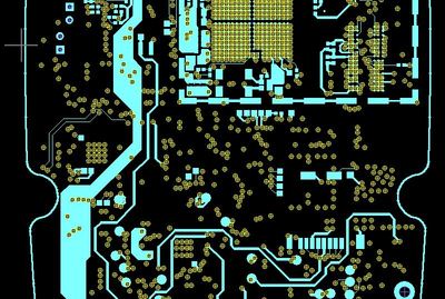
PCB Gerber
The Gerber format is an open 2D binary vector image file format. It is the standard file used by printed circuit board (PCB) industry software to describe the printed circuit board images: copper layers, solder mask, legend, etc. PCB manufacturers are able to produce bare PCB according to the Gerber files provided.
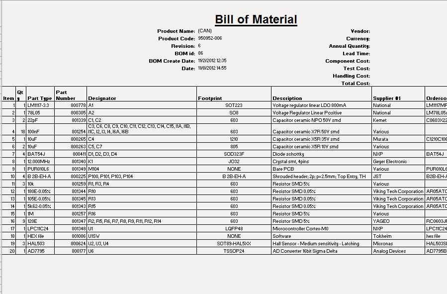
PCB BOM List
In the case of a PCB design, the bill of materials is a list of all the parts needed to build that specific printed circuit board. Normally, all the components mounted on PCB module will be take off from the PCB bare board. The location of the each component will be recorded, and models with quantities will be listed in the BOM list. The BOM list is be provided to customers finally for PCB module Copy.
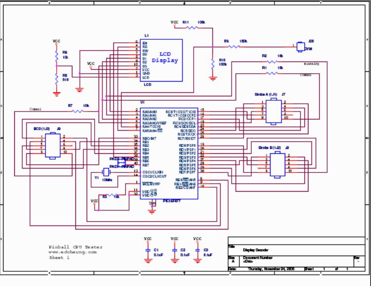
Schematics
A schematic diagram is a convenient and informative method for documenting electronic circuitry. The basic building blocks of schematic diagrams use a set of standardized symbols to represent different component types. Fast PCB Studio engineers will reverse the schematic diagram according to the PCB module received. The Schematic diagram is to be provided to customers for future uses, e.g. PCB module modification for production version upgrade.
Legal Boundary of PCB Reverse Engineering
Reverse engineering technology plays an importance role in the development of integrated circuit industry. However, since the birth of the entire concept, it has been widely in argued for its legitimacy.
Reverse engineering is committed to the second development of the original product design ideas, through the circuit analysis and data extraction, product design, adding new design concepts and functional modules, based on the original product to achieve rapid innovation and update Replacement, help enhance the overall competitiveness of the electronics industry.
January 2007 China’s Supreme People’s Court promulgated the “Interpretation on Several Issues Concerning the Application of Law in the Trial of Unfair Competition in Civil Cases,” stipulating that trade secrets obtained by means of self-development or reverse engineering shall not be deemed as relevant to the Unfair Competition Law The provisions of the violation of trade secrets.
The judicial interpretation also stipulates that reverse engineering refers to the technical means obtained from the open channel demolition of products, mapping, analysis and access to the product of the technical information. After the parties know the commercial secrets of others by improper means, they also advocate that the act of acquisition is lawful and not supported on the ground of reverse engineering.
The judicial interpretation of the February 1, 2007 came into effect.
Reverse engineering plays an important role in the development of integrated circuit industry. Since the birth of the entire concept, its legitimate has been widely argued.
So far, many Reverse Engineering Organizations have stated that all clients who requesting reverse engineering from a company must have a legal design copyright source statement in order to protect the legitimate rights and interests of the original design copyright holder, and the customers are required to promise to utilize the results for teaching, analysis, technical research and other legitimate uses.
****************************************************************************************
Reverse engineering technologies applying on teaching; analyzing and evaluating the concept, technology or layout used in the layout design, the layout of the circuit, the logic structure, the component layout and copy layout design and the analysis and evaluation results are applied to the original layout Design or manufacturing integrated circuits accordingly, are not considered infringement. However, the production of integrated circuits by simply copying a protected layout design of others for the purpose of marketing is considered a tort.
Disclaimer: The use of our reverse engineering technologies is strictly limited within legal purposes, e.g. reproduce PCB artworks for old or obsolete printed circuit boards where the original is no longer available, PCB & Design tutorial or research and etc. Fast PCB Studio would not be responsible for any legal disputes for any inappropriate use of our technology on commercial competition, patent duplication or other prohibited use of reverse engineering technology by local laws.